
PCB Design Assembly Important in Electronics
Printed circuit boards (PCBs) are a vital component in every electronic device that requires intricate, yet compact, circuitry. From the smallest smartwatch to the largest smartphone, PCBs provide a way for complex and interconnected electronic devices to function properly and efficiently. Without a PCB, your electronic device would be a mess of wires that can easily get tangled or damaged. Modern PCBs also use fewer components than traditional point-to-point wiring methods, leading to smaller devices that are more portable and easier to maintain.
A PCB is an electrical substrate with copper traces that connect to other components. These components can be either through-hole or surface mount. Through-hole components have pins that pass through holes drilled in the board, while surface mount components have small pads that are attached to the PCB with melted solder. Both types of components connect to the traces through solder pads, which are referred to as “vias.” Via sizes and types are specified in the PCB design to ensure adequate current carrying capacity and avoid short circuits.
The bare copper surfaces on the pcb design assembly dissipate heat from the components, which is an important function since electronics generate quite a bit of it. This helps the device stay cool, which is particularly helpful in environments that are not ideal for electronics, such as automobiles or medical equipment. PCBs are also durable and long-lasting, making them suitable for a wide range of applications.
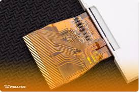
Why is PCB Design Assembly Important in Electronics?
To produce a high-quality PCB, it is essential to consider all the factors that go into the design. This includes component placement, signal integrity, and other considerations that are crucial to the performance of your final product. For example, it’s important to place the most critical components, such as the CPU, battery holder, and RTC module, on the top side of the board to maximize space efficiency. This also minimizes vibration and shock, as well as electromagnetic interference (EMI) and susceptibility issues.
Other considerations include proper clearance between components to prevent solder bridging, which can lead to a short circuit. It’s also important to have proper spacing between a component’s pads and traces, as well as the annular ring around a via hole, so that solder can make a good connection and withstand the manufacturing process. It’s also important to design for manufacturability by ensuring that all the required components are available, the correct sizes of the PCB, and the appropriate tools and equipment for assembly.
It’s also a good idea to create a layout that is easy to test and debug, as well as follow environmental regulations, such as RoHS and lead-free design. This can help reduce the risk of failure during production and enable a more robust, reliable end-product. Taking these steps early in the design process also helps to accelerate the time-to-market of your finished product.