
calculate the bend allowance for flexible PCBs
In flexible PCBs, determining the bend allowance is one of the most critical design processes. If a board is bent beyond the recommended limits it can cause failure and damage the flex circuit. In this blog post, we’ll explain why calculating the bend radius is so important and provide a step-by-step guide to figuring it out.
The Bend Allowance is the minimum radius that a flexible pcb can safely bend without damage or structural failure. The amount of bending that can be safely done will depend on the material, thickness and number of layers. Generally speaking, the greater the bend radius, the less likely it is that the circuit board will be damaged.
A good starting point for determining the bend radius is to consult with the flexible PCB manufacturer. They should have information on the mechanical properties of their materials, such as tensile strength, yield strength and elastic modulus. They can also provide guidelines for determining the minimum bend radius based on the thickness of the substrate and the number of layers of the soft or hard flex circuit board.
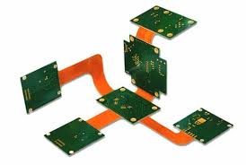
How do you calculate the bend allowance for flexible PCBs?
Whether or not you are working with an existing flex circuit board design or are starting from scratch, you’ll want to ensure that the bend radius is appropriate for your application. Incorrect bending can cause damage to the copper wires and/or plated through holes. This is especially true for repeated bending that can lead to fatigue cracking of the copper.
To avoid these problems, it’s a good idea to use thin copper traces for areas that are going to be subjected to repeated bending. This will reduce the stress on the copper and improve flex circuit reliability. In addition, it’s a good idea to stagger the placement of traces on the plane layers. This will help to eliminate the “I-beaming” effect that can increase stress on the flex circuit.
Advances in photolithography, a technique used to transfer circuit patterns onto the substrate, have played a crucial role in improving the quality and reliability of flexible PCBs. Modern photolithography processes allow for the creation of finer circuit patterns, which is essential for the production of high-density flexible PCBs used in applications like smartphones and medical devices. Additionally, innovations in etching techniques have enabled the production of thinner copper traces, further enhancing the flexibility and performance of the board.
For more severe bending applications, you may want to consider using stiffeners in your flex circuit design. Stiffeners are rigid parts that are laminated to the flex circuit board in key locations. For example, the stiffener can be placed in the area of the edge connector or mounting holes on a flex circuit board. This will add some rigidity to those areas of the flex circuit, which will reduce dynamic bending stresses and prevent the board from tearing.